NOTE: This disposition is nonprecedential. United States Court of Appeals
for the Federal Circuit
NETLIST, INC.,
Appellant
v.
MICRON TECHNOLOGY, INC., MICRON
SEMICONDUCTOR PRODUCTS, INC., MICRON
TECHNOLOGY TEXAS, LLC,
Appellees
2024-2240, 2024-2241
Appeals from the United States Patent and Trademark Office, Patent Trial and Appeal Board in Nos. IPR2022-01427, IPR2022-01428, IPR2023-00882, IPR2023-00883.
Decided: September 2, 2026
JEFFREY A. LAMKEN, MoloLamken LLP, Washington, DC, argued for appellant. Also represented by JENNIFER ELIZABETH FISCHELL, KAYVON GHAYOUMI, RAYINER HASHEM, LIDIYA MISHCHENKO; ELIZABETH KATHLEEN CLARKE, Chicago, IL; CATHERINE MARTINEZ, New York, NY.
2MICHAEL RUECKHEIM, King & Spalding LLP, San Francisco, CA, for appellees. Also represented by JUAN C. YAQUIAN, Houston, TX.
Before REYNA, LINN, and STARK, Circuit Judges.
Netlist Inc. (“Netlist”) appeals from two consolidated final written decisions of the Patent Trial and Appeal Board (“Board”), which together held unpatentable all claims of U.S. Patent Nos. 8,787,060 (“’060 patent”) and 9,318,160 (“’160 patent”). We affirm.
I
A
Netlist’s ’060 and ’160 patents generally relate to computer memory modules, such as the one depicted below. Appx10310. Some background about this technology is necessary to understand the parties’ dispute.
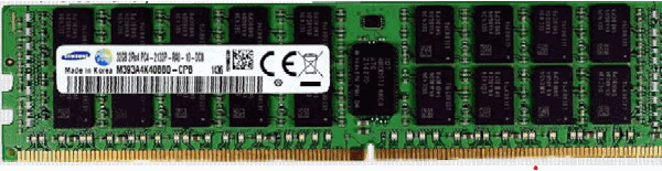
Computer memory modules store memory as dynamic random-access memory (“DRAM”) within “memory packages.” The memory module shown above contains 18 memory packages (black rectangles) organized in two rows.
The capacity of a memory module can be increased by adding additional memory packages. Additionally, as described in the ’060 and ’160 patents, capacity can be increased by using three-dimensional stack (“3DS”) memory packages. A 3DS memory package contains multiple3 silicon “array dies” on top of one another. The 3DS approach is roughly analogous to adding stories to a building. Figure 1B of the ’060 patent illustrates one such 3DS arrangement as well as additional concepts pertinent to 3DS memory packages and this appeal. Appx150 (annotations added by Netlist).

This figure shows a memory package 150 containing four array dies 160 (blue) stacked atop a single “control die” 170 (red). Appx181 (1:62-66). “Die interconnects” 182 and 188 (vertical black lines), which may take the form of “through-silicon vias” (“TSVs),” connect the array dies to the control die. Appx181 at 2:2-7; Appx181 at 1:35-49; Appx183 at 5:51-54.
Figure 1B also shows that the control die (red) includes “drivers” 184 and 186 (grey triangles). The drivers push electrical signals through the interconnects to each array die.
4While increasing the number of array dies increases the capacity of the memory package and, therefore, the memory module, doing so also has drawbacks. As more array dies are stacked, the control die drivers experience greater “load,” a physical phenomenon the control die must overcome in order to send a signal to the array dies. The load increases as more dies are added to the interconnects and as the interconnects are made longer.Consequently, greater loads require larger drivers, which take up valuable space on the control die and consume more energy.
B
Netlist’s ’060 and ’160 patents share a specification and priority date. Their titles are “Method and Apparatus for Optimizing Driver Load in a Memory Package” and “Memory Package with Optimized Driver Load and Method of Operation,” respectively. Appx171, Appx147. Both patents purport to teach “methods for reducing the load” in memory modules that utilize three-dimensional stacking. Appx181 at 1:19-22. Netlist’s patents claim to reduce load by altering how array dies are connected to the control die. Specifically, the patents manage the amount of load by reducing the number of array dies connected to each interconnect and reducing the length of at least some of the interconnects.
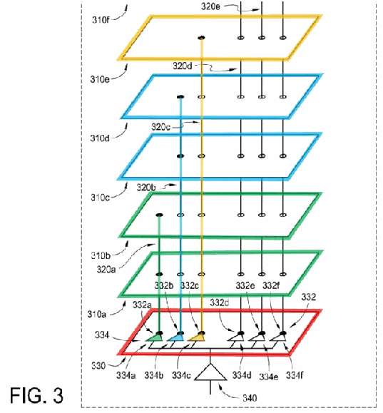
5Figure 3 of the ’060 patent illustrates an embodiment of Netlist’s claimed invention. Appx175 (cropped and annotated by Netlist). The control die 330 is outlined in red, while the groups of array dies are shown in green (310a and 310b), blue (310c and 310d), and yellow (310e). Darkened circles, such as 332a and 332b, indicate electrical connections between an interconnect running from the control die to an array die; unfilled circles show where an interconnect passes through a hole in an array die without making any connection.
As Figure 3 is intended to illustrate, Netlist’s invention uses interconnects that do not connect to all array dies in a stack. The resulting smaller number of connections, and shorter interconnects, reduces the load the drivers (e.g., 334a, 334b, and 334c) need to overcome.
Claim 1 of the ’060 patent is representative of all independent claims at issue in this appeal and recites:
6A memory package, comprising:
a plurality of input/output terminals via which the memory package communicates data and control/address signals with one or more external devices; a plurality of stacked array dies including a first group of array dies and a second group of at least one array die, each array die having data ports; at least a first die interconnect and a second die interconnect, the first die interconnect in electrical communication with the first group of array dies and not in electrical communication with the second group of at least one array die, the second die interconnect in electrical communication with the second group of at least one array die and not in electrical communication with the first group of array dies; and a control die comprising at least a first data conduit between the first die interconnect and a first terminal of the plurality of input/output terminals, and at least a second data conduit between the second die interconnect and the first terminal, the first terminal being a data terminal, the control die further comprising a control circuit to control respective states of the first data conduit and the second data conduit in response to control signals received via one or more second terminals of the plurality of terminals.
Appx192 (emphasis added).
Two dependent claims are also at issue. Claim 7 depends from claim 1 and adds that the number of array dies7 in each group “are selected in consideration of a load of the first die interconnect and a load of the second die interconnect so as to reduce a difference” in load. Appx192. Claim 15, which depends from independent claim 11 (which, as pertinent to this appeal, is identical to claim 1), adds a requirement of “a first driver having a first driver size, and . . . a second driver having a second driver size.” Appx193.
C
The petitions for inter partes review challenged all claims of both the ’060 and ’160 patents.1 Appellees allege the claims would have been obvious over various prior art combinations. The references at issue on appeal are: (1) Patent Application Pub. No. 2011/0103156 (“Kim”), which discloses a stacked memory module in which array dies are connected to a control die by a TSV; (2) U.S. Patent No. 8,041,881 (“Rajan”), which teaches attaching groups of DRAM dies (referred to in Rajan as “chips”2) using a single data bus; (3) U.S. Patent No. 7,969,192 (“Wyman”), which discloses that different length TSVs require different8 amounts of power, i.e., draw different load, as well as a driver with multiple taps that can provide different amounts of power; and (4) U.S. Patent Application Pub. No. 2011/0026293 (“Riho”), which teaches connecting array dies to a control die through TSVs.
The Board instituted the petitions and ultimately found all claims of both patents unpatentable as obvious. Netlist then timely appealed. The Board had jurisdiction under 35 U.S.C. §§ 314, 318(a). We have jurisdiction under 28 U.S.C. § 1295(a)(4)(A) and 35 U.S.C. §§ 141(c), 319.
II
We review the Board’s legal determinations de novo and its underlying factual findings for substantial evidence. See Neptune Generics, LLC v. Eli Lilly & Co., 921 F.3d 1372, 1375 (Fed. Cir. 2019). Obviousness is a question of law based on underlying facts. See id. Whether a person of ordinary skill in the art would have a motivation to combine or modify references and have a reasonable expectation of success in doing so, are questions of fact. See PAR Pharm., Inc. v. TWI Pharms., Inc., 773 F.3d 1186, 1193, 1196-97 (Fed. Cir. 2014).
Claim construction based solely on intrinsic evidence is an issue of law we review de novo. See HTC Corp. v. Cellular Commc’ns Equip., LLC, 877 F.3d 1361, 1367 (Fed. Cir. 2017). We likewise accord de novo review to allegations that the Board failed to comply with its obligations under the Administrative Procedure Act (“APA”), 5 U.S.C. § 706. See Axonics, Inc. v. Medtronic, Inc., 75 F.4th 1374, 1380 (Fed. Cir. 2023).
III
Netlist raises several issues on appeal. First, it argues that the Board erred in finding a skilled artisan would have been motivated to combine Kim and Rajan to arrive at9 claim 1 of the ’060 patent.3 Next, Netlist faults the Board’s findings that Appellees proved claims 7 and 15 of the ’060 patent obvious. Finally, Netlist asserts that the Board violated the APA by failing to adequately explain its reasoning with respect to certain limitations. We discuss, and reject, each of these contentions below.
A
Claim 1 of the ’060 patent requires first and second groups of array dies electrically connected to a first and second die interconnect, and that the interconnect for the first group be electrically connected to that first group but not to the second group while the interconnect for the second group is electrically connected to the second group but not the first. Netlist argues that a skilled artisan would not have been motivated to combine Kim and Rajan to reach this limitation. We are not persuaded.
The Board explained: “Petitioner’s combination is a straightforward one – implement a shared data bus for multiple memory chips as taught by Rajan . . . using, e.g., Kim’s TSV interconnects.” Appx99-100 (internal quotation marks omitted). In the Board’s view, a person of ordinary skill in the art would have been motivated to combine Rajan’s shared data bus for multiple memory chips with Kim’s TSV interconnects because “Kim suggests having more than two dies, Rajan discloses how to share a data bus among multiple dies, and the evidence of record shows that TSVs were used to implement data busses.” Appx100-01. The Board further found that, in adding dies, a skilled artisan would have followed Rajan’s approach of adding10 multiple dies to Kim’s TSVs because it would have avoided the need to create additional TSVs, “which would add space and circuitry.” J.A. 101. Substantial evidence, including the disclosures of Kim and Rajan cited by the Board, supports these findings. See, e.g., Appx101 (citing Appx2009 at ¶164; Appx3631-32 at ¶¶ 48, 50; Appx4649 at 1:39-42, 2:56-64).
In challenging the Board’s motivation to combine finding, Netlist raises a multitude of complaints, none of which have merit. Netlist argues that Kim teaches away from multiple array dies being connected to a single die interconnect, insisting that instead Kim is limited to what it calls a “one-to-one correspondence;” i.e., each array die is on its own die interconnect. Open. Br. at 17 (citing Appx3629 at ¶ 17). The Board thoroughly considered this contention and cited substantial evidence for rejecting it, including Kim’s statement that “any number of . . . chips may be used.” Appx93 (quoting Appx3631 at ¶ 48). Moreover, even if Kim discloses a one-to-one relationship between array dies and TSVs, that does not mean that a skilled artisan would read Kim as teaching away from a single TSV connecting to multiple array dies. See Meiresonne v. Google, Inc., 849 F.3d 1379, 1382 (Fed. Cir. 2017) (“A reference that merely expresses a general preference for an alternative invention but does not criticize, discredit, or otherwise discourage investigation into the claimed invention does not teach away.”) (internal quotation marks omitted).
Netlist also faults the Board for failing to recognize that the combination of Kim and Rajan “[e]viscerate[s] Kim’s [i]nvention and [p]urpose,” which is a memory device where a centralized I/O circuit is shared by all array dies. Open. Br. at 43-44.. According to Netlist, the combination’s “removal of the I/O circuit from the [array] dies, and use of a shared I/O circuit, threatens fatal data collisions.” Open. Br. at 44 (internal quotation marks and alterations omitted). The Board addressed this concern head on. The11 Board had substantial evidence for its findings that Rajan “explains how to avoid collisions through the timing of various operations,” Appx105-06 (citing Appx3651-57, Appx3664-66 at 8:59-12:13), and that a person of ordinary skill in the art “knew how to deal with collisions,” including through familiarity with certain industry standards (such as the Joint Electron Devices Engineering Council or “JEDEC,” which is mentioned in Netlist’s patents), Appx102, Appx105-06.4
Netlist next argues that the Board’s identified motivation to combine, i.e, adding array dies, was generic and, therefore, inadequate. See Appx93; see also ActiveVideo Nets., Inc. v. Verizon Commc’ns, Inc., 694 F.3d 1312, 1328 (Fed. Cir. 2012) (rejecting motivation “to build something better” as generic and insufficient to reverse jury finding of motivation to combine). But the Board relied on Kim’s express disclosure that “any number of . . . chips may be used,” Appx93 (citing Appx3631 at ¶48), and found that a skilled artisan would “‘look at Rajan for the details about adding more memory chips in the stack,’” Appx93, which we conclude is a sufficiently specific motivation to combine.
Lastly, Netlist asserts that the Board violated the APA by failing to adequately address certain of its arguments. The APA requires the Board to identify the reasons for reaching its conclusions and their bases in record evidence. See Alacritech, Inc. v. Intel Corp., 966 F.3d 1367, 1370 (Fed. Cir. 2020). “We do not require perfect explanations, and we will uphold a decision of less than ideal clarity if the agency’s path may reasonably be discerned.” Id. (internal quotation marks omitted).
12The Board satisfied these standards. We have reasonably discerned the Board’s reasons for rejecting Netlist’s motivation to combine contentions, which we have discussed (and found supported by substantial evidence) above. To the extent Netlist identifies among its many arguments some that the Board did not explicitly analyze, this was not error here, as “[t]he Board is not required to address every argument raised by a party or explain every possible reason supporting its conclusion.” Novartis AG v. Torrent Pharms. Ltd., 853 F.3d 1316, 1328 (Fed. Cir. 2017) (internal quotation marks and alterations omitted).
Thus, we reject Netlist’s challenge to the Board’s conclusion that claim 1 of the ’060 patent was proven unpatentable as obvious.
B
Netlist disputes the Board’s determination that claim 7 of the ’060 patent was obvious over the combination of Kim, Rajan, and Riho. Claim 7 requires that a “number of array dies” in the first and second groups be “selected in consideration of” the load of the respective die interconnects, “so as to reduce a difference between a first load on the first data conduit and a second load on the second data conduit.” Appx192 at 24:37-47. The Board found that Riho “discloses using . . . equal length TSVs” and “an equal number of dies in each group,” and thus “teach[es] . . . considering load when grouping dies.” Appx125.
While neither party asked the Board to construe any term relating to claim 7, Netlist now contends that the Board erred by implicitly construing claim 7 as not requiring a difference in loads as a starting point. Netlist asserts that a difference in load comes from having different length TSVs. Even assuming this is a non-forfeited claim construction position, we agree with the Board that the claims are not limited to different-length TSVs. What is required is that load difference be given consideration, which can be done even when that difference is zero.
13Thus, substantial evidence supports the Board’s findings underlying its conclusion that claim 7 was proven obvious.
C
Netlist also appeals the Board’s determination that the combination of Kim, Rajan, and Wyman renders obvious claim 15 of the ’060 patent. In particular, Netlist attacks the Board’s finding that these references disclose a “first driver” with a “first driver size” and a “second driver” with a different “second driver size.” The Board found that Wyman teaches “physically separate drivers can be used to provide . . . different amounts of signal drive.” Appx134. The Board relied on Appellees’ expert, who opined that a skilled artisan would know “you can provide a separate copy of [Wyman’s] circuit 500 for each thing that needs to be driven after you analyze the current requirements.” Appx132 (quoting Appx6984 at 129:2-7). This is substantial evidence for the Board’s findings.
D
Finally, Netlist argues that the Board violated the APA by not adequately addressing every limitation of every challenged patent claim. It particularly faults the Board’s handling of limitations to which Netlist raised no dispute; for these limitations, the Board merely summarized Appellees’ contentions, noted that Netlist did not dispute them, and indicated it was persuaded by Appellees. See, e.g., Appx120 (“Patent Owner does not raise additional arguments for these claims. We have reviewed Petitioner’s arguments and evidence, and we find them persuasive”).
Netlist raised this precise argument in a related appeal, Netlist, Inc. v. Micron Technology Inc., No. 24-1859 (Fed. Cir. Sept. 2, 2026). Our opinion in that case, which we are issuing concurrently with this opinion, addresses and rejects Netlist’s position. For the same reasons given14 there, we are likewise unpersuaded by Netlist’s critique here.
IV
We have considered Netlist’s remaining arguments and find them unpersuasive. Accordingly, for the reasons given above, the judgment of the Board is affirmed.
AFFIRMED
Footnotes
- ↩ 1 Samsung Electronics Co., Ltd. (“Samsung”) filed petitions for inter partes review challenging all claims of the ’060 and ’160 patents IPR2022-01428; IPR2022-01427. Micron Technology, Inc., Micron Semiconductor Products, Inc., and Micron Technology Texas, LLC (collectively, “Micron”) filed similar petitions, challenging the same claims based on identical invalidity theories. IPR2023-00882; IPR2023-00883. Micron and Samsung’s petitions for each respective patent were consolidated before the Board. Appx1; Appx69. Samsung has since settled with Netlist and withdrawn from this appeal. This opinion therefore refers to Micron as “Appellees.”
- ↩ 2 For purposes of this appeal, the terms “chip” and “die” have the same meaning. See Appx166 at 18:45-48; Appx2075.
- ↩ 3 For ease of reference, this section only discusses the ’060 patent. The same analysis also applies to the ’160 patent because, as discussed, claims 1, 7, and 15 of both patents (and the Board’s analysis of those claims) are identical in all respects relevant to the disputes on appeal.
- ↩ 4 For these reasons, Netlist’s similar suggestion that a skilled artisan would lack a reasonable expectation of success from the combination of Kim and Rajan also fails.